Circuit Design Tutorial
Contents
Circuit for Signal Logic
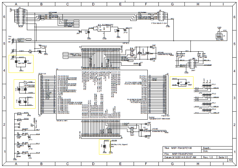
The yellow boxes highlight the circuits that were to be implemented on our PCB so that the MSP432 micro-controller could communicate with the single-board computer and the motors.
Power Requirements
Current and voltage ratings were obtained from the links below. The max current value for the XL-320 was obtained experimentally as 0.45A, but 0.6A was used for a safety margin.
XL-320: Datasheet
AX-12: Datasheet
MX-28: Datasheet
MX-64: Datasheet
MX-106: Datasheet
Voltage Regulation
Linear regulators are easy to use since they often only require two external resistors and two capacitors to set the output voltage, however they are very inefficient in terms of efficiency. Linear regulators typically have efficiencies in the fortieth percentile range. They take the difference between the input voltage and output voltage and dissipate that energy as heat. This not only wastes power, but it also can generate heat, which, if not removed, can damage the board.
Switching regulators solve this efficiency setback with the trade-off of a more complicated external circuit. Switching regulators typically have efficiencies in the eightieth percentile range. They achieve this by taking moving energy from the input to the output, bit by bit. This is done with a switch and controller.
Before selecting electrical components, I highly recommend looking at the PCB guide provided by Dr. Pachowicz (http://ece.gmu.edu/~ppach/ECE492-3/Resources/Seminar-PCB.pdf).
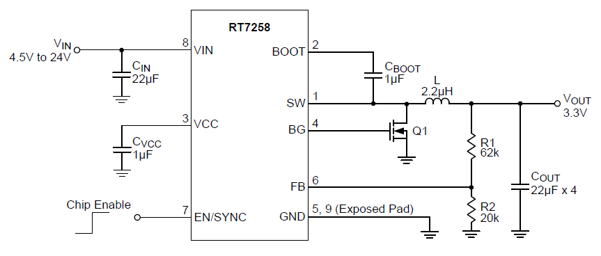
The regulator that was selected was the RT7258. This regulator was selected because out of the recommended chip packages that are easily surface mounted by hand, it provided the most current (8 amps). The datasheet can be found here: http://www.richtek.com/assets/product_file/RT7258/DS7258-01.pdf .
Having selected the regulator, the necessary quantity of regulators can be calculated from the current requirements:
In addition to the quantities seen above, two regulators will be needed to supply a 3.3V and 5V rail for the single board computer and micro-controller.
Setting the Output Voltage
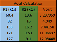
The above circuit is for a 3.3V output, but the output can be adjusted by using different values for R1 and R2:
For selecting resistors, it is good practice to choose a tolerance of 1%. Standard 1% resistor values can be found here: http://www.rfcafe.com/references/electrical/resistor-values.htm.
Inductance Calculation
Enable Input Resistor Network
The chip needs a voltage signal (2V < EN < 5.5V) to enable operation. Allowing for a power supply to range from 15V to 24V, R1 = 390 ohms and R2 = 100 ohms yields (3.06V < EN < 4.89V)
The selection of all other components for the regulator do not require calculations and the datasheet offers straightforward guidance on selecting proper components.
Over-Voltage Protection
TVS diodes were connected in parallel (reverse-bias) with the output voltage going into the motors. When the diode sees a voltage level higher than its rated breakdown voltage, the diode creates a short circuit to ground to protect the motor. To select the proper diode, choose the diode with Vwm set to the maximum allowable voltage of the circuit. For more on TVS diode selection please see: http://www.completepowerelectronics.com/tvs-diode-selection-tutorial/ .
Over-Current Protection
Fuses were used to protect the motors from any unexpected harmful surges of current. The fuse rating for each.
Reverse Polarity Protection
Often when motors reverse direction, they can induce a reverse current, which if it feeds into the board can damage the components. To prevent this, a P-Channel MOSFET will be used. The MOSFET is superior to the standard diode used for reverse polarity protection because the MOSFET only consumes a negligible voltage during operation as opposed to the diode which can draw 0.7V~1.2V from the output. More information on reverse polarity protection can be found here:http://www.ti.com/lit/an/slva139/slva139.pdf
Status LED's
To easily identify blown fuses or damaged components, status LED’s were incorporated into the design. Most LED’s are designed for a current of ~20ma. To find the proper resistor to place in series to achieve this current, the following formula was used:
Connectors
Terminal blocks were used to connect the power supply to the board. Multiple blocks were used to limit the amount of current flowing through any one trace, since traces can only handle a certain amount of current.
Attaching pin headers to the board allows for the PCB board to connect to the motors. With crimps placed on the ends of wires and inserted their appropriate housings, they can easily connect to the board.
Power Relay
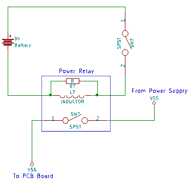
Standard on/off switches cannot handle loads of current on the order of 50+ amperes. This is where a power relay comes in to act as the on/off switch:
Using a standard switch and a 9V battery you can control the current through the inductor in the relay to open or close the connection from the power supply to the PCB board.
PCB Design
As mentioned earlier, it is very important to read through Dr. Pachowicz PCB design guide (http://ece.gmu.edu/~ppach/ECE492-3/Resources/Seminar-PCB.pdf) to ensure your design can be manufactured in-house at GMU.
Additionally I recommend going through the following tutorials to obtain a better understanding of how KiCAD works:
http://teholabs.com/knowledge/kicad.html
http://docs.kicad-pcb.org/en/getting_started_in_kicad.html
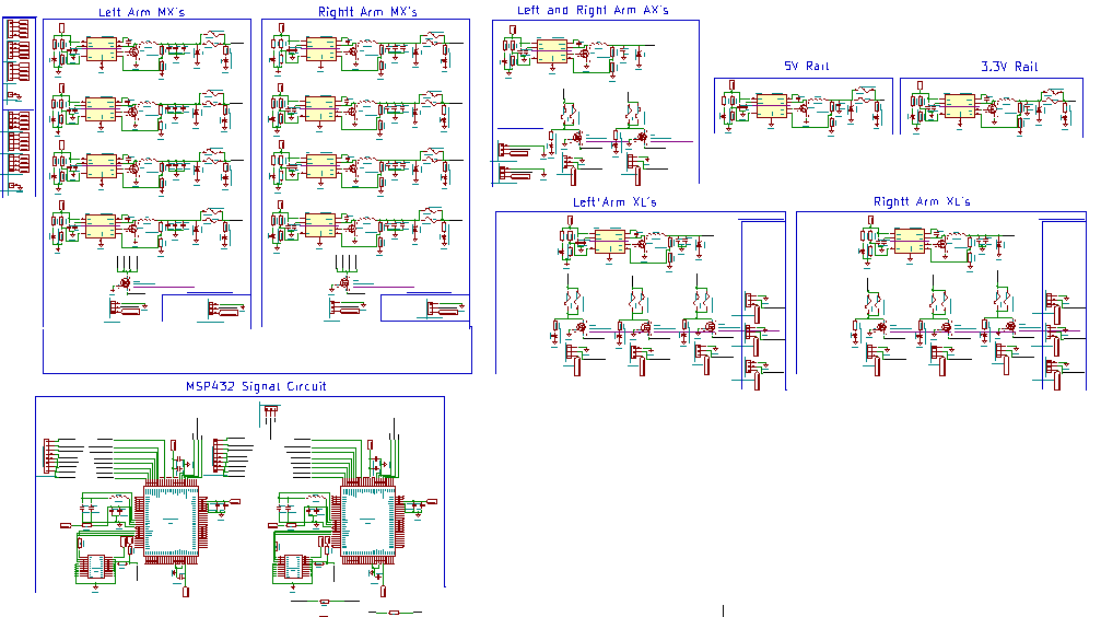
The first step to PCB design is to make a working schematic:
On the far left are the power inputs into the board. There are 12 power supply inputs and 1 ground input. The 12 inputs can be broken down as (8x12V rail, 1x11.1V rail, 2x7.4V, 1x3.3V&5V). The more current a particular rail draws the more important it is to divide the current into separate traces, rather than having 1 large bulky trace. The 11.1V rails and 3.3V&5V rails don’t draw large current loads, which is why fewer power inputs connections (traces) can be used.
Ground only has one port because the entire back layer will be used as a ground plane. Thus trace width is not a concern.
Beneath the 13 power ports, you will see the same 13 ports mirrored. This is because PCB fabrication at GMU does not have plated through-hole capability. Thus you must add mirrored holes for all through-hole parts, so that you can solder a wire through the board to make the connection. Using surface mount technology (SMT) avoids this, plus smaller components lead to smaller board size, but be careful not to get anything too small because then they can become difficult to solder by hand. Dr. Pachowicz’s PCB guide addresses this issues of the workarounds for through hole technology and lists certain electronic SMD packages that able to be soldered by hand.
The left arm and right arm each use 4x12V regulators. A TVS diode, fuse, and status LED is connected to the output of each regulator and on the input of each regulator is a status LED. The reason why each arm uses 4x12V regulators is due to the large current load that each arm can draw.
You may notice that there are pairs of fuses in the schematic. One is a real fuse, the second serves to act as mirrored holes since the fuse is a through-hole component. The output of each of the four regulators feeds into the P-CH MOSFET, which is present to prevent reverse current from flowing into the board. Below the MOSFET is the pin header for the left-arm 12V rail.
The circuit for the 12V rail for the right arm is set-up in the same manner.
The 11.1 V rail only requires 3A so 1 regulator can be used. The 11.1V output was split into two pin headers since each arm requires their respective signal.
Similarly the left hand and right hand can each be powered by one regulator. Each hand has three fingers which requires three pin headers per hand.
The bottom left corner holds the circuit for the signal logic. Some signals were linked to 0 ohm resistors. This is so that traces can jump other traces on the PCB Board Layout.
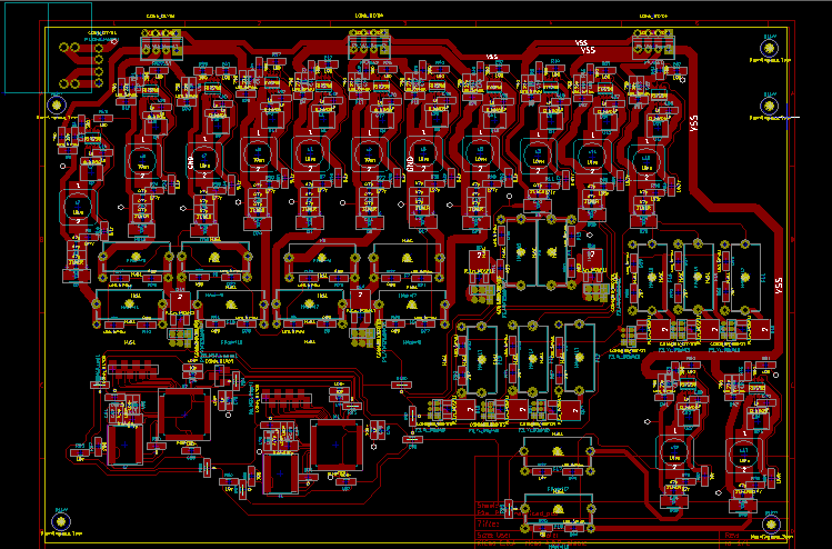
Once the schematic is done, then you must associate footprints with components. Once that is done, then you can begin to lay the PCB tracks. When laying tracks, try to make all angles 45 degrees and make sure the trace width is rated for the amount of current that will run through the track. This link will calculate the required trace width based on design specifications: http://www.circuitcalculator.com/wordpress/2006/01/31/pcb-trace-width-calculator/
Future Improvements
The board size is approximately 8in .x 11in., meaning the board is extremely large. One improvement that could be made to decrease the board size is to modularize the voltage regulators. This could be done by simply making a small board for a 12V, 11.1V, 7.4V, etc. and attaching pins to the small board so that it could plug into a pin socket on the larger board with the other components. When a regulator breaks down the circuit could be remedied by simply unplugging the faulty regulator and inserting a new one.
Files
Circuit Bill of Materials and Calculations: https://github.com/ASL-Robot/pcb-design/blob/master/PCB_BOM.xlsx
PCB Board Files: https://github.com/ASL-Robot/pcb-design/tree/master/PCBFinal
